


_final.jpg/_jcr_content/renditions/Mkgaa32x18.jpeg)
_final.jpg)
Select your Market
{{ userContent.title }}

This webinar is hosted by SEMI EMG and sponsored by the Electronics business of Merck KGaA, Darmstadt, Germany.
Virtual Event
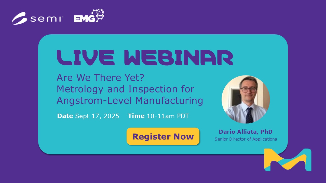
17 Sep 2025
Enabled by optical intelligence
Enhancing Manufacturing Yield Performance for Heterogeneous 3D Packaging in AI Devices.
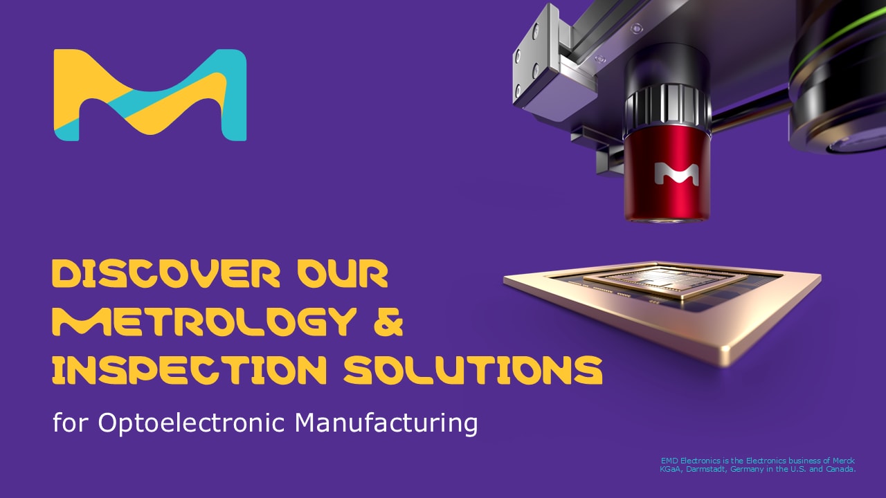
Metrology and Inspection for Angstrom-Level Manufacturing
In the semiconductor industry where we routinely pattern sub-wavelength structures and require atomic-layer precision in our manufacturing processes, it’s easy to assume that we can simply measure everything we’re doing and all the structures we create. In reality, though, metrology and inspection have the challenging task of not just keeping up with device technology but staying far enough ahead that we can actually “see” our results and confirm the progress we’re making.
In this webinar, we will explore the metrology and inspection space to learn more about technological advances driving this vital segment of semiconductor manufacturing.
The webinar will feature presentations by Dario Alliata, Ph.D, Sr. Application Director for Metrology & Inspection.
Following the presentations, an interactive Q&A segment will allow attendees a chance to deepen their understanding of how materials innovation and advanced metrology intersect at the leading edge of manufacturing.
Join us to engage with peers and pioneers working at the forefront of materials science and semiconductor innovation!
The massive adoption of social networking and artificial intelligence has pushed the semiconductor industry to develop devices capable of supporting the required infrastructures. Increasingly powerful computer process units (CPU) are used to allow data centers to process trillions of information exchanges, while faster graphic process units (GPU) enable virtual and assisted reality.
Cost leveraging is now reachable with the integration of multiple dies in the same package, each one fabricated to handle specific functionalities with the most cost-effective technology node, which is a form of heterogeneous integration. This session highlights some examples of metrology and inspection solutions aimed at securing the manufacturability of devices for High Computing Power fundamental for AI applications. More in detail, it explores the challenge of the fabrication of chip-to-chip interconnections that are key for the heterogeneous integration of active components with vertical stacking like DRAM for High Bandwidth memories, where process tolerances are increasingly narrow and conditions to measure more and more extremes.

Senior Director of Applications
The Role & the Challenge of Metrology and Inspection in Advanced Packaging of AI Chips
17 Sep 2025
Dr. Dario Alliata joined Unity-SC, now part of the Electronics business of Merck KGaA, Darmstadt, Germany in the U.S. and Canada. In 2016 as product manager and is now Sr. Director of Applications with focus on Advanced packaging and Specialty substrates & devices. He worked in the semiconductor industry for more than 25 years, initially in R&D centers and later in equipment makers. He spent his entire career developing process control solutions for securing the manufacturing chain in the semiconductor industry. He received a MD in Physics from the University of Milan (Italy) and hold a Ph.D. in Physics & Chemistry from the University of Berne (Switzerland).
Watch our free on-demand webinars to explore pressing topics on materials and semiconductor development. Click here to get more information.
_2nd-webinar.jpg/_jcr_content/renditions/Mkgaa32x18.jpeg)
_2nd-webinar.jpg)
_3rd%20webinar_rv3.jpg/_jcr_content/renditions/Mkgaa32x18.jpeg)
_3rd webinar_rv3.jpg)