Select your Market
-
{{ userContent.title }}

{{ userContent.lookingForMoreLabel }}


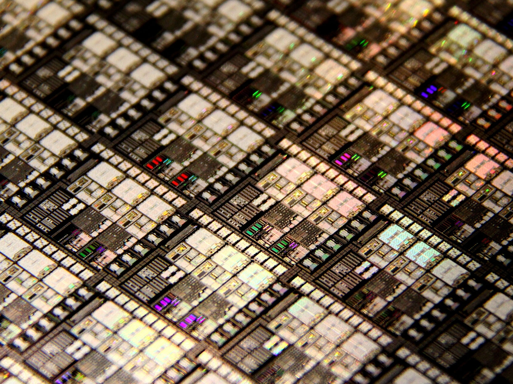
Formulations
Innovative formulations driving precision, reliability, and performance in semiconductors.
Advanced Formulation Solutions
We are uniquely positioned to drive innovation in semiconductor manufacturing with a comprehensive portfolio of formulations that enhance the efficiency, precision, and reliability of electronic devices.
Our offerings encompass a wide range of technologies, including advanced patterning, chemical mechanical planarization, and cleaning solutions. Each formulation is meticulously designed to meet the evolving demands of the industry, ensuring optimal performance across various applications.
By leveraging our expertise in materials science, we empower our customers to navigate the complexities of semiconductor fabrication and achieve their production goals.
-

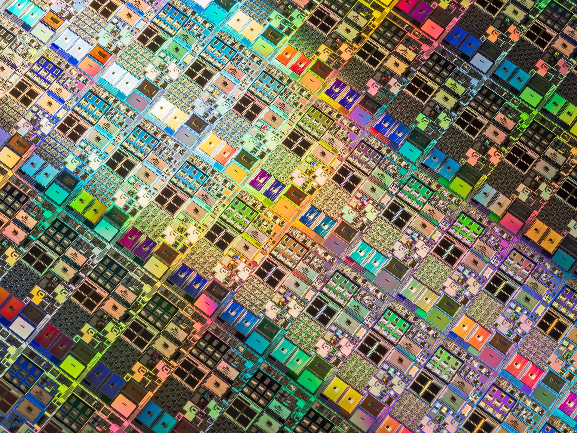
Patterning
ExplorePatterning transfers intricate designs onto semiconductor wafers using photolithography. Our formulations—photoresists, antireflective coatings, and developers—are essential for creating precise circuit patterns, ensuring every detail is captured flawlessly.
-

Planarization
ExploreAchieving a smooth surface on wafers is crucial for performance. Our chemical-mechanical planarization (CMP) formulations use specialized slurries to remove excess material, creating a flat surface that prevents electrical issues.
-

Cleans
ExploreOur cleaning formulations ensure pristine wafer surfaces before processing. They effectively remove contaminants and residues, preparing high-quality surfaces for layering and etching, enhancing overall device performance.