



Select your Market
-
- Algeria
- Angola
- Benin
- Botswana
- Burkina Faso
- Burundi
- Cameroon
- Cape Verde
- Central African Republic
- Chad
- Comoros
- Congo
- Congo Democratic Republic
- Djibouti
- Egypt
- Equatorial Guinea
- Eritrea
- Ethiopia
- Gabon
- Gambia
- Ghana
- Guinea
- Guinea-Bissau
- Ivory Coast
- Kenya
- Lesotho
- Liberia
- Libya
- Madagascar
- Malawi
- Mauritania
- Mauritius
- Morocco
- Mozambique
- Namibia
- Niger
- Nigeria
- Reunion Islands
- Rwanda
- Saint Helena
- São Tomé and Príncipe
- Senegal
- Seychelles
- Sierra Leone
- Somalia
- South Africa
- Sudan
- Swaziland
- Tanzania
- Togo
- Tunisia
- Uganda
- Zambia
- Zimbabwe
-
- Albania
- Austria
- Baltic Region
- Belarus
- Belgium
- Bulgaria
- Croatia
- Cyprus
- Czech Republic
- Denmark
- Estonia
- Finland
- France
- Germany
- Greece
- Hungary
- Ireland
- Italy
- Latvia
- Lithuania
- Luxembourg
- Netherlands
- North Macedonia
- Norway
- Poland
- Portugal
- Romania
- Russian Federation
- Serbia
- Slovakia
- Slovenia
- Spain
- Sweden
- Switzerland
- Türkiye
- Ukraine
- United Kingdom
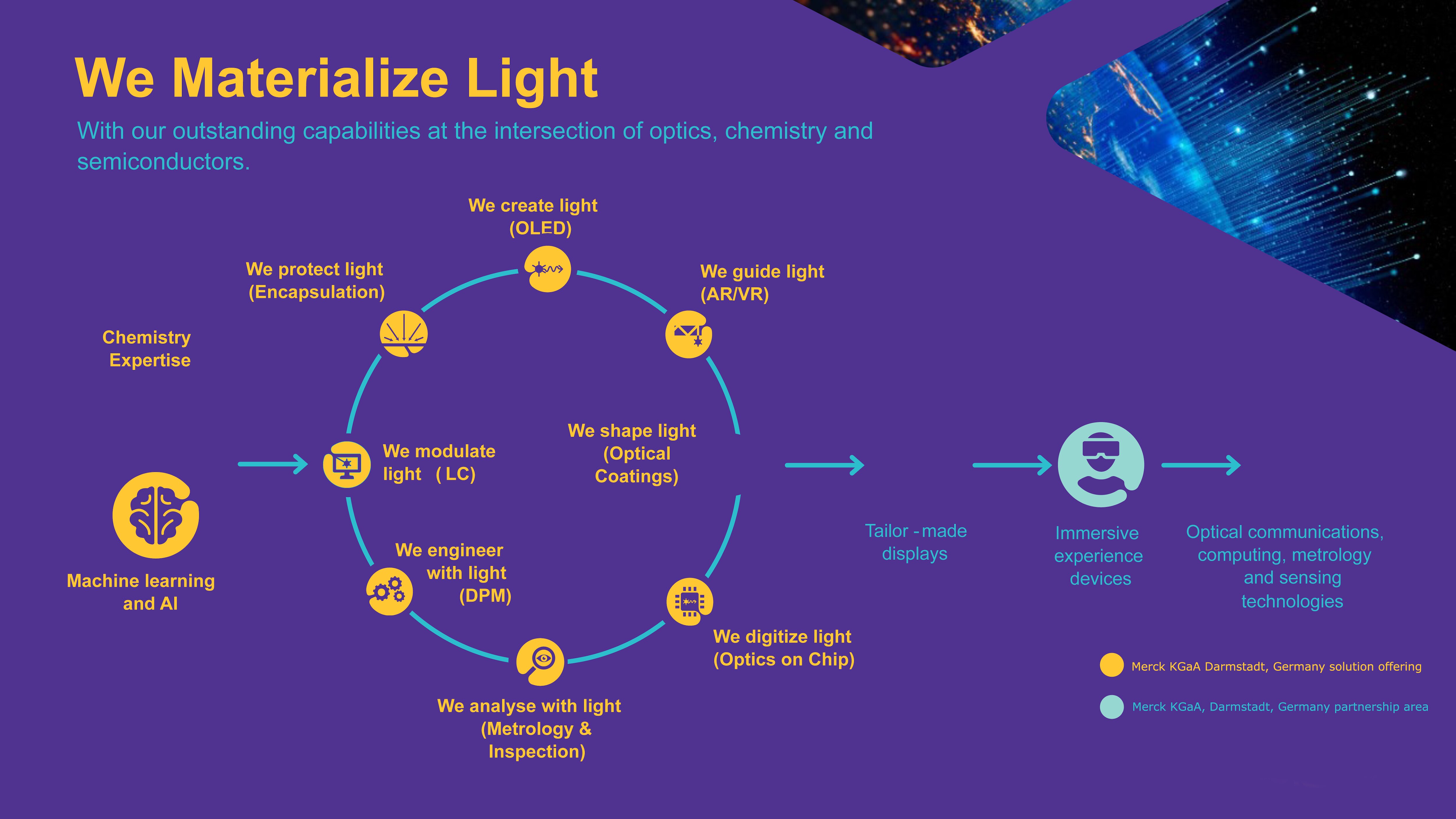
How we materialize light
Light is an essential part of our daily lives, from the formation of rainbows to the growth of plants through photosynthesis. It illuminates our world and brings color and energy to everything around us.
Innovation for high-performance applications
We harness the transformative power of light to reshape the landscape of electronic devices and systems.
driving the future of electronics
Merck KGaA, Darmstadt, Germany Electronics' Optronics business exemplifies innovation for high-performance applications with its profound commitment to the principle "We Materialize Light", demonstrating our comprehensive mastery over the fundamental elements of light manipulation.
Situated at the intersection of advanced chemistry, optics, display and semiconductor technology, our business is uniquely positioned to address the growing demands for immersive digital experien ces across electronics.

What we do –
Our Solutions
Building on more than 120 years of expertise in LC technologies, we have broadened our leadership into the realm of AR/VR and semiconductor metrology, developing next-generation materials and technologies.
Our expertise has been organized into three distinct clusters, each dedicated to innovating how we interact with the fundamental properties of light: Display Materials, Optical Technologies and Metrology & Inspection.


Display Materials
As a leading-edge supplier in Liquid Crystals (LC) and Organic Light Emitting Diodes (OLED) materials we have revolutionized the way light is created and modulated in displays.
We modulate light with Liquid Crystals
LC materials can be finely adjusted to respond to external stimuli, such as electric fields and temperature, making them integral to advanced displays and optical devices. These materials enable the modulation of light for various purposes, from high-resolution displays to optical switches and photonic integrated devices.
learn more
We protect light with Encapsulation Materials
Encapsulation materials are developed to create a protective layer for the sensitive layers in OLED Display stacks, shielding them from moisture and oxygen. Our low-temperature ALD silicon materials offer highly improved barrier characteristics.
learn more
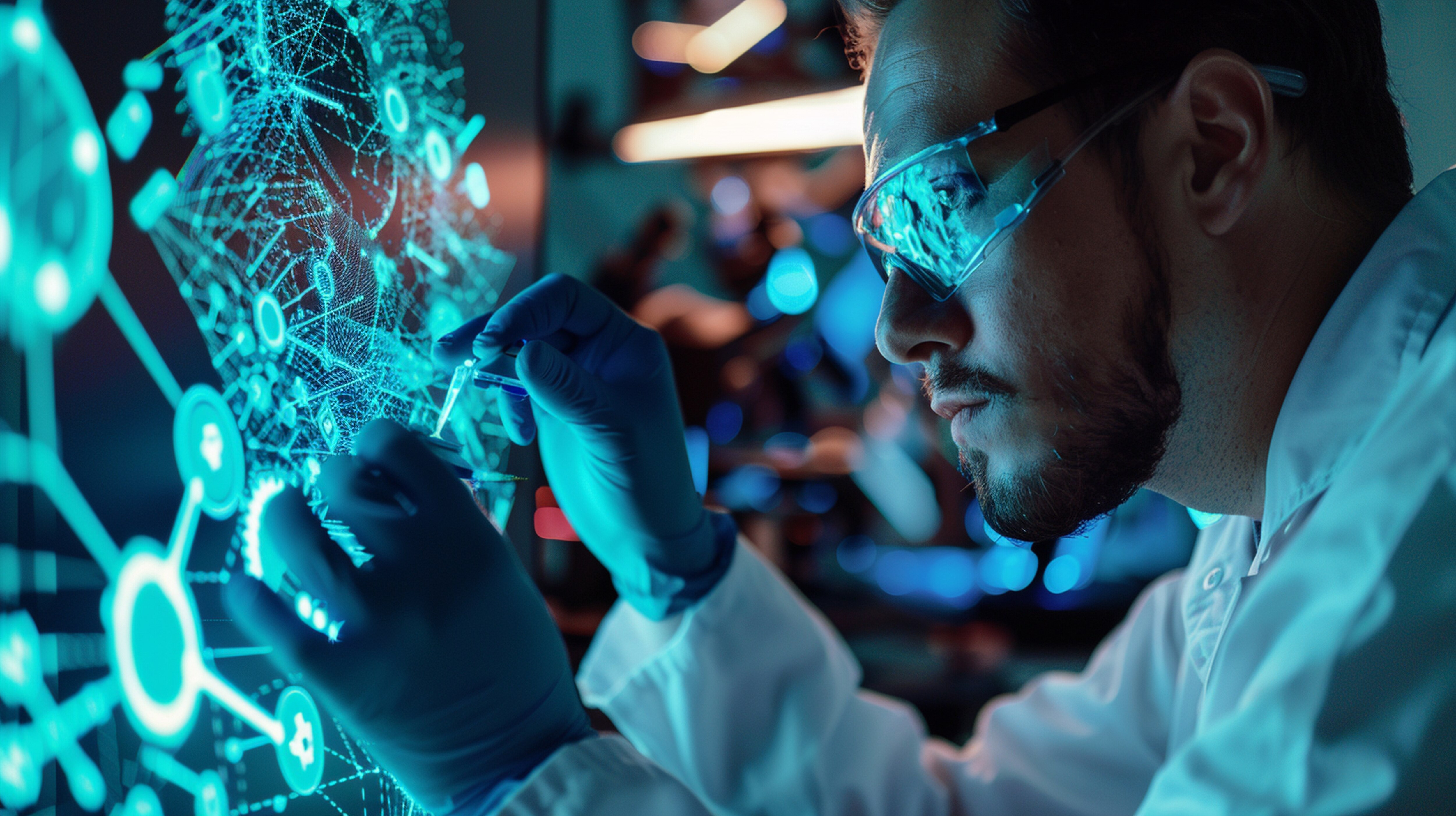
Optical Technologies
By manipulating light with high precision, optronics technology is enabling the development of devices tailored to specific use cases across multiple industries, improving the way we interact with digital content and environments.

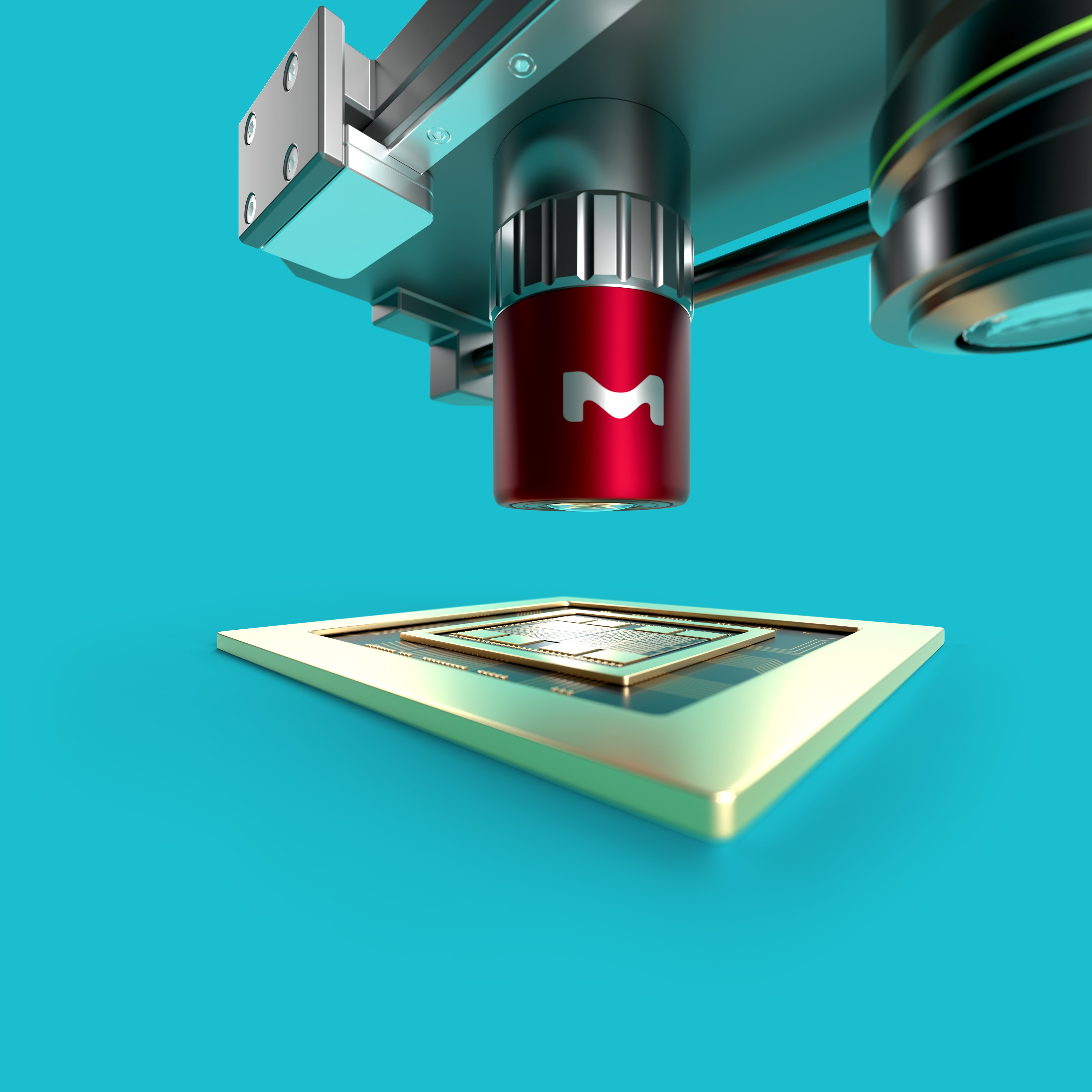
Metrology and Inspection
Our ability to control and measure light and understand its interactions with various semiconductor industry materials is the area in which Merck KGaA, Darmstadt, Germany excels.
We analyze with light
Our metrology & inspection capabilities have expanded to include the most advanced tools available for opto-electronic manufacturing. These tools provide high-precision measurements critical for semiconductor processes, including wafer geometry control, defect detection, and surface analysis. By combining our specialized optronics knowledge with cutting-edge metrology & inspection, we create unique synergies that enrich our portfolio.
learn more

Overall, light is crucial…
in enhancing the performance, efficiency, and visual quality of new optical technologies, advanced displays and semiconductor devices, driving innovation in these fields.
Our expertise in light and matter interaction for optical and electronic materials, along with our pioneering work in LC and OLED, positions us to lead in integrating optical components into semi devices. This allows us to serve a diverse range of customers, from optical tech and display panel makers to semiconductor manufacturers.
textblock default title
“Our deep expertise in the design of the interaction of light and matter related to both optical and electronic materials, combined with our pioneering work in liquid crystal and OLED technologies, positions us uniquely to lead in the integration of optical components into semiconductor devices. This dual focus allows us to serve a wide range of customers, from optical technologies and display panel makers to semiconductor manufacturers. “