


-
Advancing the Dry Etching Process
Join us to discover how to advance your dry etching process by building a robust supply chain and driving material innovation. This webinar is co-hosted by SEMI.
Learn More -
Overcoming EUV Lithography Barriers Through DSA Technology
The complex molecular assembly of DSA will be explained, and we will walk through the steps of how it can be integrated into an advanced patterning process. This webinar is co-hosted by SEMI.
Learn More -
Scaling Digital Solutions
Join us to discover how data and strengthening digital technologies is one of the top priorities for semiconductor businesses to address higher yields, zero defects, and shrinking dimensions.
Learn More -
Advanced Materials
Learn how to best introduce new materials in chip fabrication workflows as the demand for better performance, functionality, and reliability grows for applications such as 5G, AI/VR, AR & edge computing.
Learn More -
New Standards for Semiconductor Materials
Join us to discover how digital solutions are forming new ways of operating in a fast-paced, highly demanding semiconductor industry. This webinar series is co-hosted by SEMI.
Learn More -
Innovations in ALD and ALE
Join us to discover how innovations in selective surface-controlled processes, including Atomic Layer Deposition (ALD) and Atomic Layer Etch (ALE), enable the manufacture of advanced electronic devices.
Learn More
Select your Market
-
{{ userContent.title }}

{{ userContent.lookingForMoreLabel }}
Spin on Dielectric
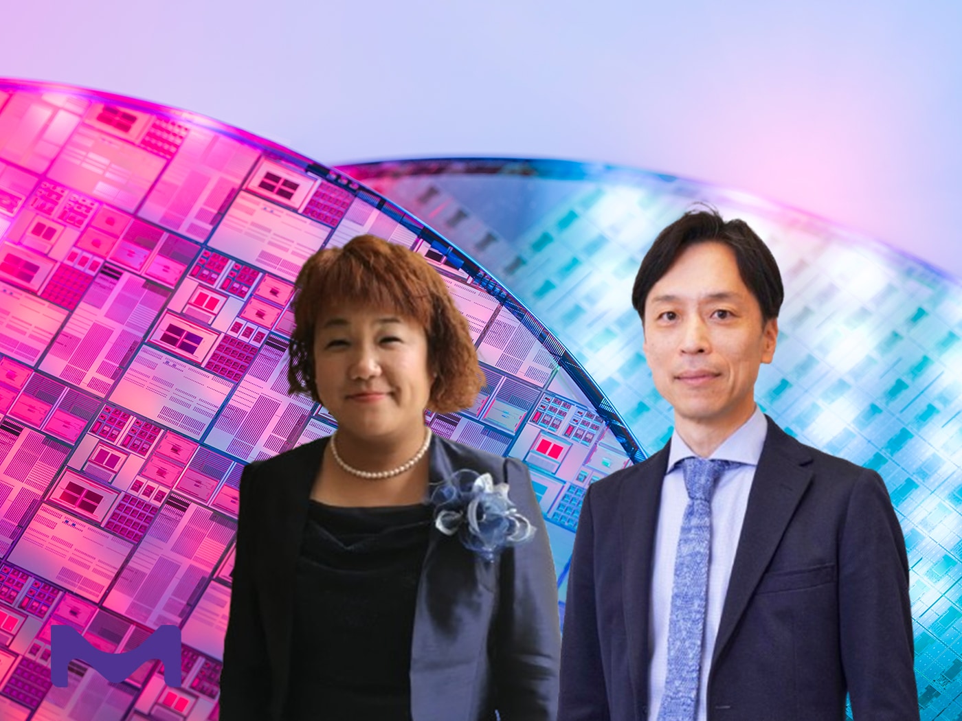
Presentation by Atsuko Yamamoto, R&D Manager & Go Nakano, Spin-on Global Marketing Manager
Watch On-demand
Join us to discover how Spin-on Dielectrics (SOD) materials and processes contributed to advanced semiconductor device manufacturing, and new material development to overcome future device challenges.
Agenda
October 23, 2024 | 10:00 am - 11:00 am CET
10:00 am CET - Welcome remarks by Laith Altimime | President, SEMI Europe & Surésh Rajaraman | Executive Vice President and Head of Thin Film
10:10 am CET - Semiconductor Device Process Evolution by Spin on Dielectric by Atsuko Yamamoto | R&D Manager, Spin-On Dielectric & Go Nakano | Spin-on Global Marketing Manager
10:50 am CET - Q&A Moderated by Laith Altimime and Conclusions by all speakeres | President, SEMI Europe & Executive Vice President
Speaker
Atsuko Yamamoto | R&D Manager, Spin-On Dielectric
Atsuko Yamamoto is the manager of R&D in Semiconductor Materials leading the polymer research program of the Spin-On Dielectric R&D group. After joining the company in 1998, she worked as an R&D scientist of photoresist for TFT arrays, technical marketing for photo patterning materials for packaging applications in semiconductor markets and Si-based materials for optoelectronic applications. She led the R&D team in Japan and successfully launched new products as Head of display materials R&D. She is based at the R&D and manufacturing site in Kakegawa, Shizuoka-Pref. Japan.
Go Nakano | Spin-on Global Marketing Manager, Dielectric Global Marketing
Go Nakano is a Spin-on Global Marketing Manager focusing on new product development marketing of Spin-on dielectric for advanced memory and logic devices manufacturing. With more than 30 years of combined business and technical expertise in electronics-related fields, Go Nakano has a proven record of accomplishment as Head of Strategic Marketing of Display Patterning Materials, successfully led new product introduction, and expanded market share in existing products. He is based in Tokyo, Japan.
Semiconductor Materials
Contact Us
Are you interested in learning about a specific topic? Submit your topic ideas for future webinars to the Global Marketing Communications Team.