


ALD in Confined Spaces
Publish Date
14 JAN 2020
Overview
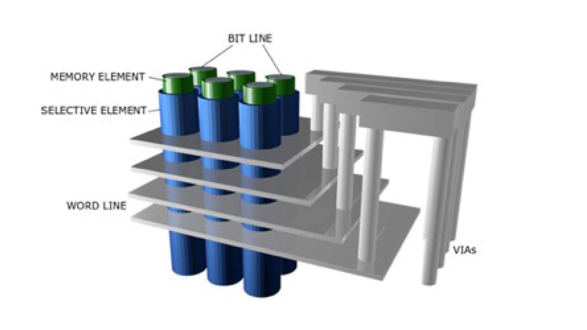
In 3D vertical memory, active and electrode materials are layered inside deep vias with aspect ratios greater than 40:1. In previous posts, we’ve talked about how atomic layer deposition (ALD), a layer-by-layer, self-saturating chemical deposition process, can fill these types of structures.
In 3D vertical memory, active and electrode materials are layered inside deep vias with aspect ratios greater than 40:1. In previous posts, we’ve talked about how atomic layer deposition (ALD), a layer-by-layer, self-saturating chemical deposition process, can fill these types of structures. In the example below, ALD deposited memory elements and selective elements run down the length of deep bit line vias: the crosspoint between each planar wordline and bit line via defines an individual memory cell.
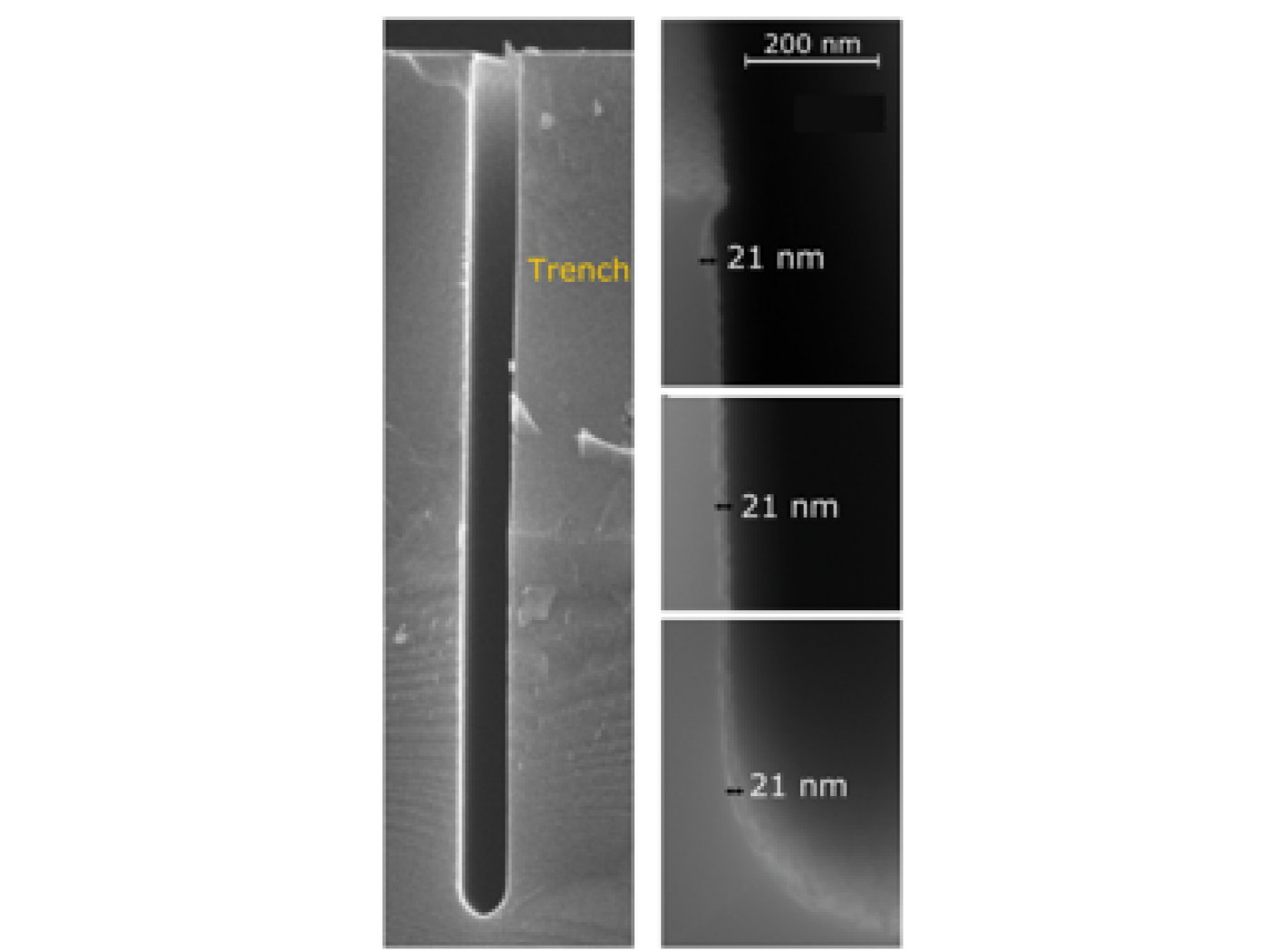
For the memory to be operable, it is critical not only for the memory and selector materials to fill the via but also to have consistent properties through its entire depth, i.e., every cell should behave the same way. The standard method for testing these properties would be to use patterned wafers with high aspect ratio structures (for example, trenches) and take cross-sectional electron micrographs to measure thickness, crystallinity, and chemical information. Sample preparation for this type of activity can be very complicated, and significant time and expense could be required for this type of measurement.
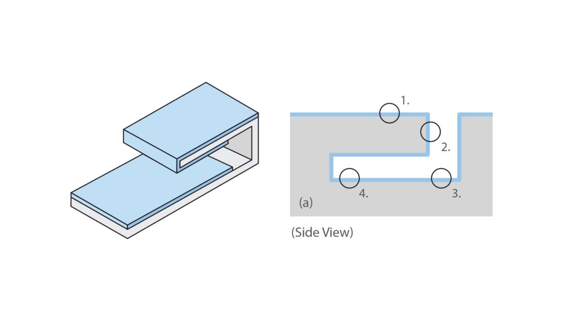
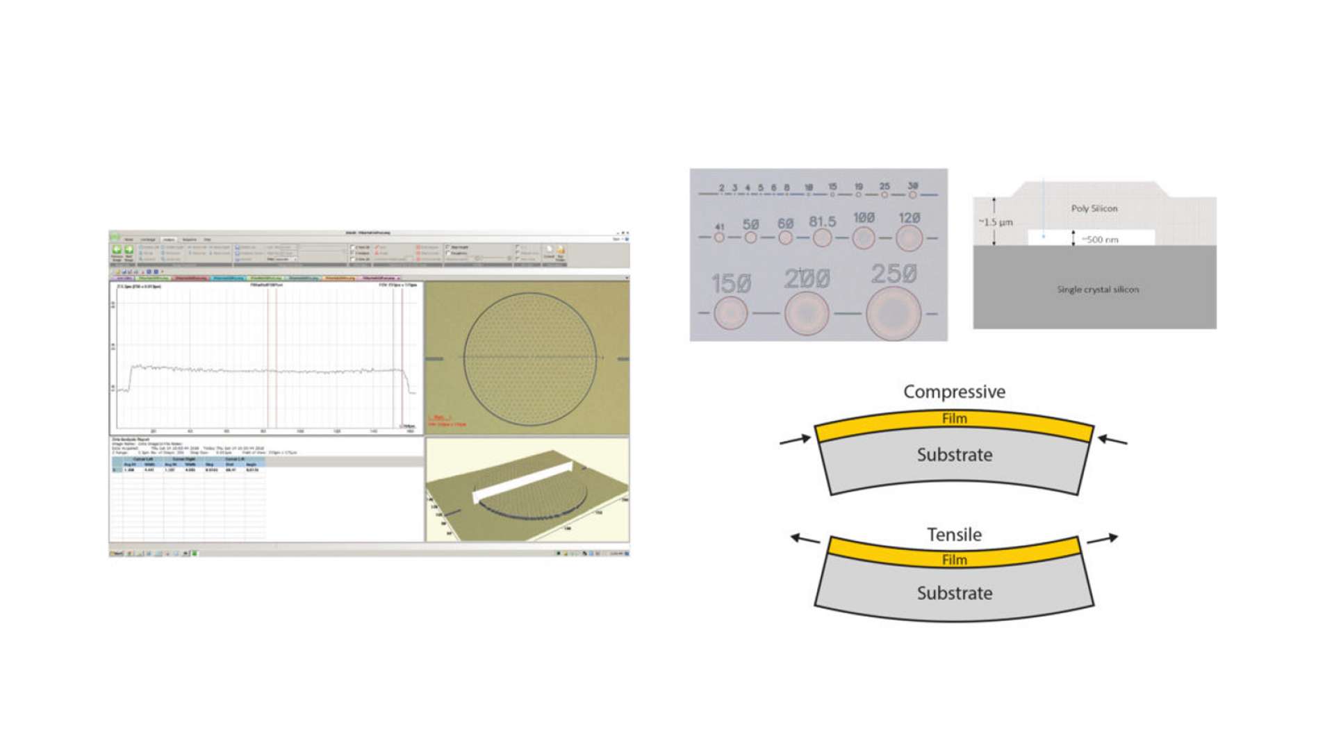
Using a platform developed by VTT Technical Research Centre of Finland, Intermolecular has developed a simpler screening method for looking at the properties of films deposited into high aspect-ratio structures. VTT’s PillarHall® chip consists of membranes suspended above a silicon substrate and supported by nanoscale pillars. These are effectively “horizontal trenches.”
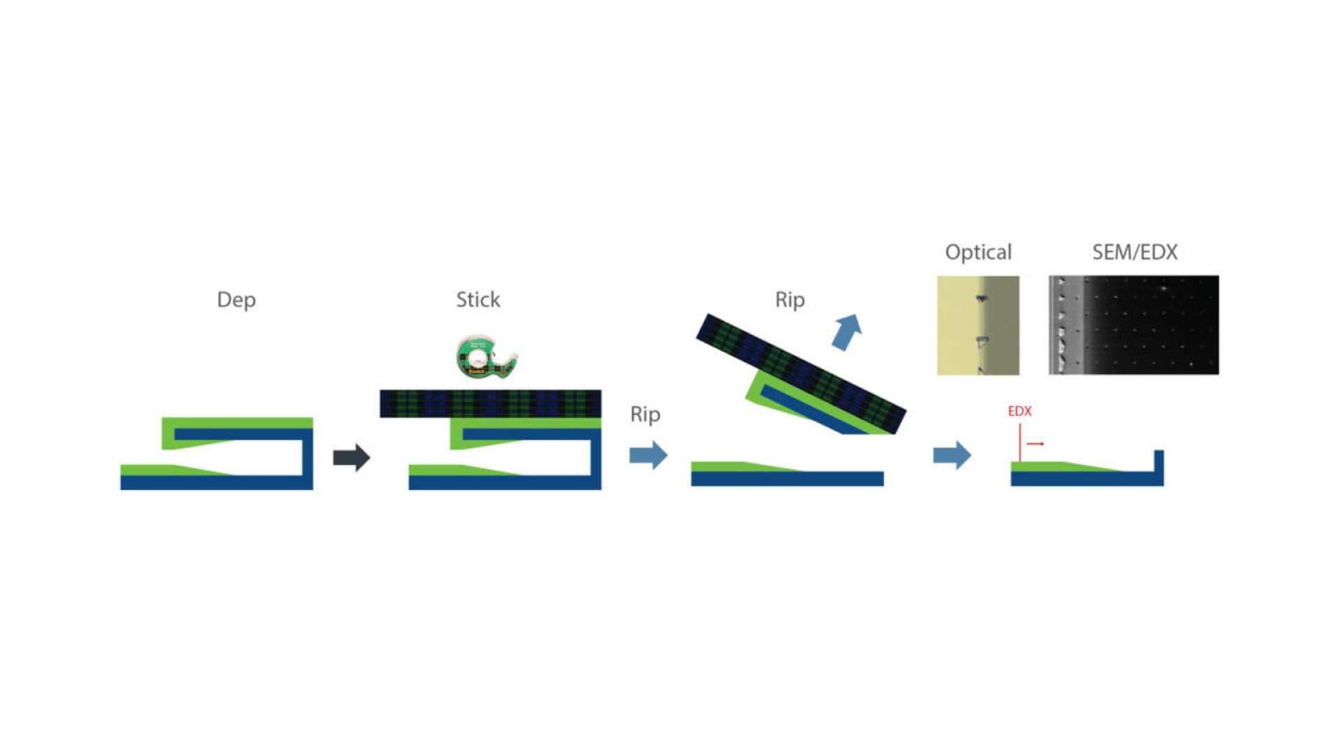
The advantage of using this type of structure is that instead of needing cross-sections, simple planar metrology techniques can be used, and sample preparation is as easy as “dep, stick, rip!” The film is deposited on the trenches by ALD, a piece of sticky tape is attached to the sample and peeled off, and then any standard planar metrology technique can be used, for example, optical microscopy or SEM/EDX.
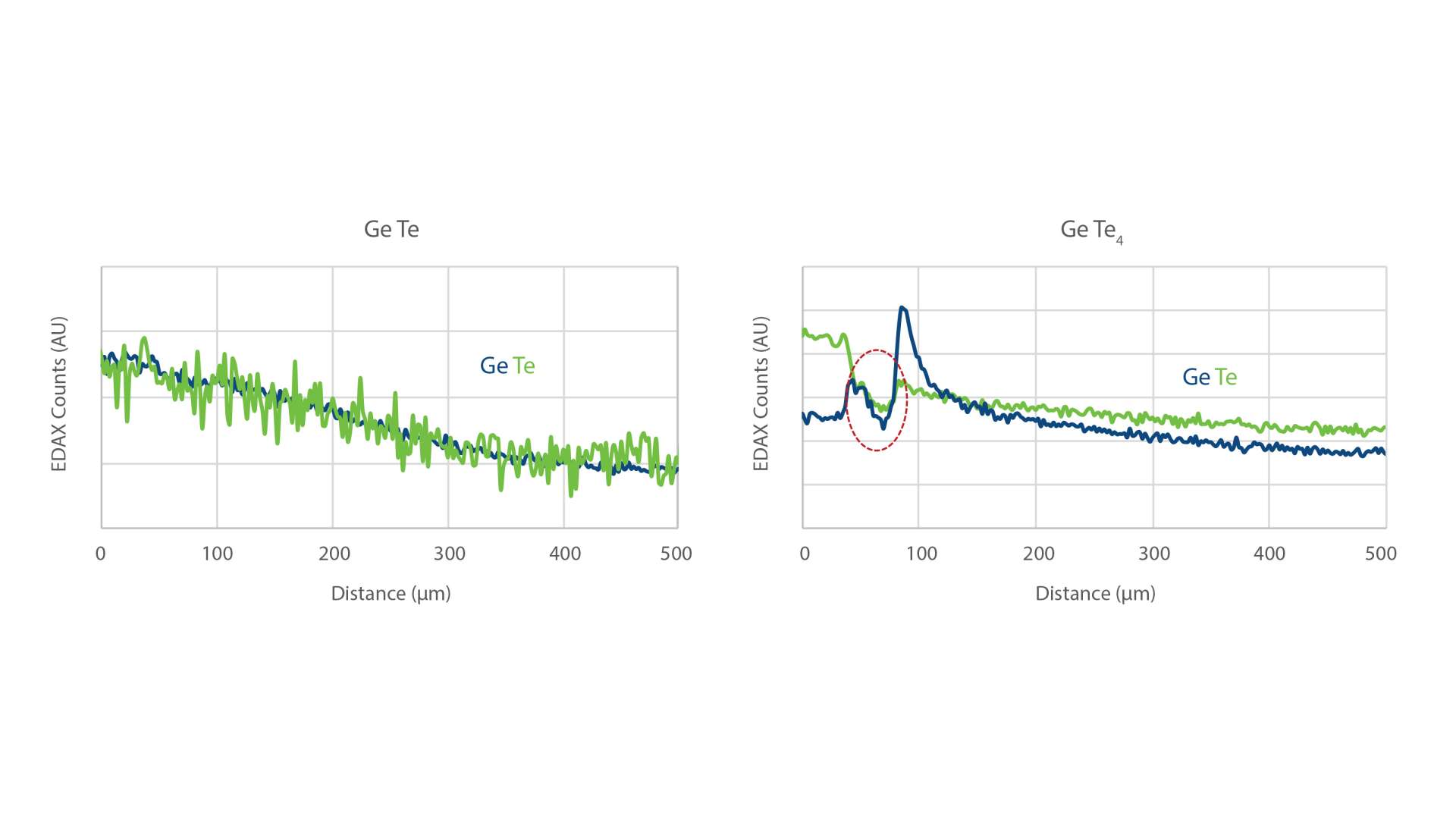
This type of analysis can be very informative, revealing behavior that would be impossible to detect using standard metrology techniques. For example, let’s look at the behavior of ALD chalcogenides, which we talked about in another post, when we deposit them inside of a deep trench. In the graphs below, we show the elemental content of a GeTex film as a function of the distance into the trench. While the equal-ratioed ALD GeTe film is relatively well behaved, a film targeted to a tellurium-rich GeTe4 composition has a highly variable elemental profile, which would mean different memory cells may behave very differently or not work at all. Detecting this type of issue with an ALD film using a simple test chip could allow for process optimization and mitigation early in the development cycle, long before it would reveal itself in a device wafer.
Beyond composition, thickness, and crystallinity, stress is an important metric for ALD films in memory applications. Excessive or mismatched stress in films can give rise to unexpected electrical properties or physical problems like film delamination. By measuring the curvature of the enclosed membranes on the PillarHall chip using a technique like optical interferometry, we can measure the film stress of each deposited film and the entire stack to detect issues before deployment in devices.
For composition, thickness, and stress, Intermolecular’s workflows on the PillarHall platform can accelerate learning about films to go beyond simple step coverage measurements and look at the detailed properties of films in high aspect ratio structures, anticipating problems early in the development process and providing detailed insights.