


Leakage Variation with Aspect Ratio in ALD High-k ZrO2 Dielectrics
Publish Date
02 NOV 2021
Overview
This blog summarizes the presentation given by Dr. Martin McBriarty on Atomic Layer Deposition in high-aspect-ratio-spaces, exploring how a material’s properties may change as the material goes into deep features and how we use a high-aspect ratio (HAR) test vehicle to investigate this behavior.
The problem at hand Industry researchers are investigating ways to scale DRAM capacitors and enable denser memory with atomic layer deposition (ALD). As we pack more capacitors onto a single chip, we see problems with scaling and the ability to preserve the capacitance of each DRAM component. Capacitance is a function of the dielectric constant and the area of the capacitor, but it’s also inversely proportional to the thickness of the dielectric material. If we want to build an optimal DRAM device, then we need a thin high-k dielectric over a large area, which we achieve by folding up the DRAM capacitors, as seen in the image below.
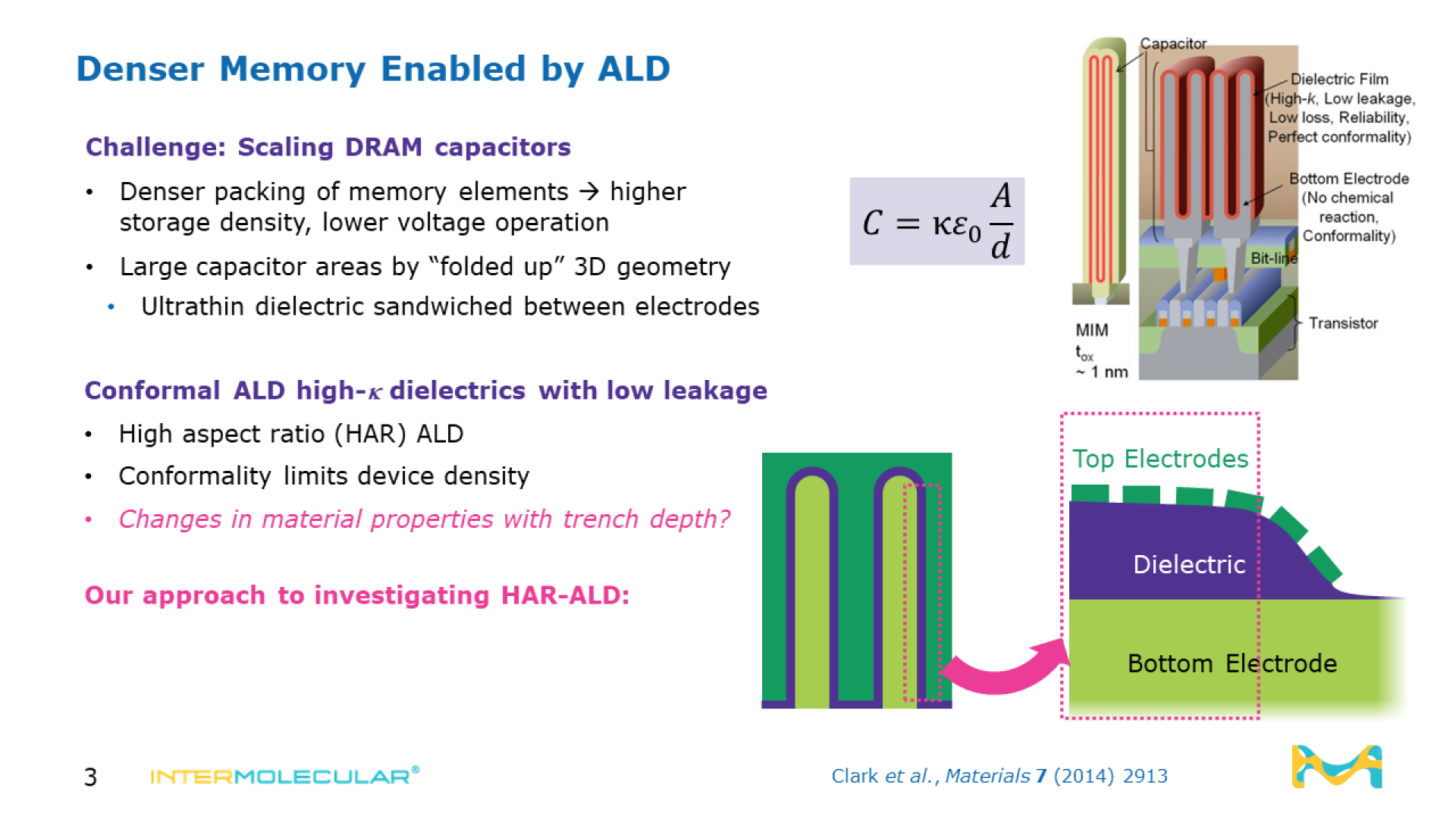
However, this folded-up geometry introduces challenges with scaling. In particular, we need to have a film that can be deposited conformally all the way down into the trench, meaning it has as similar thickness and properties as possible from top to bottom to prevent leakage. If the film is thinner at the bottom of the trench than at the top, then the whole DRAM array must be designed so the film at the bottom of the trench is thick enough, which limits the device density.
Looking down the trench At Intermolecular, we use a high-aspect ratio (HAR) test vehicle to study how the dielectric properties change along the depth of the trench. It takes the nanoscale phenomena that would happen in a real HAR device and projects these onto a scale that we can study with standard metrologies on the order of hundreds of microns to millimeters. We can then construct metal-insulator-metal capacitors (MIMcaps) along the trench to investigate the electrical properties of model DRAM devices in these hard-to-reach spaces.We start off with a flat coupon, typically a 44-millimeter square made of silicon or silicon with something deposited on top, such as a bottom electrode (BEL) material. Mono-disperse microbeads are then applied to the corners; the microbead diameter is typically chosen between 20 and 50 microns. A flat cover coupon is placed on top to form the trench. Because the microbeads are all close to a single diameter, and the coupons are flat, then we can expect that there will be even spacing between the top coupon and the bottom coupon. We can then put this “trench” structure into an ALD reactor. We choose the trench spacing (i.e. the microbead size) to ensure that the ALD process will only infiltrate part of the way toward the center of the “sandwich.”
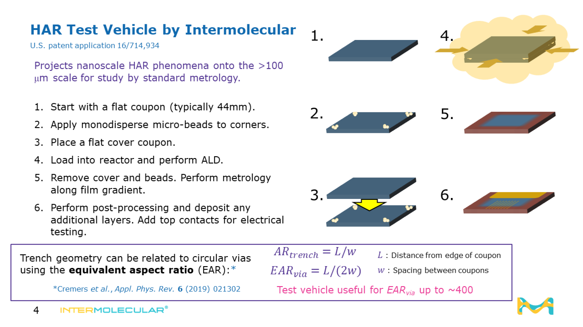
After the ALD process, we remove the top coupon and measure the thickness gradient of the film into the trench. Sometimes this gradient can even be seen by eye! Electrical testing along the gradient can be conducted after depositing a series of top electrodes that span this entire gradient area from the edge of the coupon to the center.
Testing high-k ZrO2 dielectrics To make a MIMcap using a regular open-faced or “blanket” ALD process, we start off with a silicon wafer with a thin silicon oxide layer. A layer of titanium nitride (TiN) is deposited by PVD, and zirconium oxide (ZrO2) is deposited by cycling an amide-type zirconium precursor and ozone in an ALD process at 250 °C. Another layer of TiN is deposited by PVD using a shadow mask to define top electrodes, creating individual devices to study their electrical properties. We also perform a post-metal anneal.The results of our experiments illustrated good capacitor performance: there was low leakage across the dielectric and a reasonably high dielectric constant. However, there is some asymmetry in the current-voltage curve, which could be caused by differences between the two TiN-ZrO2 interfaces in the device; specifically, the bottom TiN electrode may have been partially oxidized to titanium oxide (TiO2) during the ALD process.We can run the same experiment using our HAR-ALD test vehicle. Once again, we start with a blanket PVD bottom electrode of TiN, but then we use the HAR test vehicle to deposit ZrO2. The zirconium precursor could only infiltrate so far into the trench during its dose time, resulting in a film that extends only a few millimeters from the edge of the coupon but no film at the center of the coupon. Next, we add top electrodes in a rectangular region that spans the ZrO2 film gradient. We perform the same post-metal anneal as we did for the previous case.
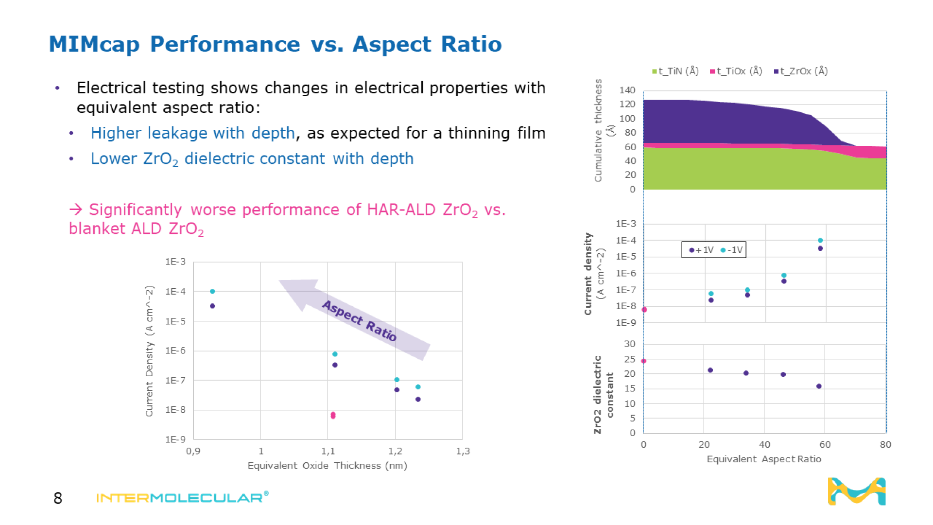
We measure the thickness of the ZrO2 film using ellipsometry. For this measurement, we assume that the top of the TiN bottom electrode has oxidized to TiO2. It turns out that as we go deeper into the film and the ZrO2 thins out, we end up with a thicker TiO2 layer. This indicates that the ozone half cycle of the ALD process oxidized the TiN deeper than the zirconium precursor was able to infiltrate.If we plot the results from both metrology and electrical testing, we see that thinner films with lower equivalent oxide thickness (EOT, as compared to a SiO2 film) result in higher leakage, as expected. Comparing the results from the HAR platform with the results of the blanket ZrO2 deposition (the magenta dots in the current-EOT plot), we see that the blanket deposition gives a much lower leakage – an order of magnitude less than for a capacitor with the same equivalent aspect ratio in the trench. This indicates there must be something fundamentally different about the deposition chemistry in these trenches.
Beyond DRAM Implementing this testing process will benefit a range of applications in 3-dimensional architectures such as in 3D NAND Flash memory and phase-change memory. In circumstances where we need to build 3D architectures and grow dielectrics and other materials very thin, ALD in HAR structures, along with complementary process methods such as atomic layer etch (ALE), will help build them inefficient and marketable ways.