


Overview
What will be the next revolution in semiconductor processing? In this blog, Martin reveals what atomic layer processes are, how thermal ALE works, and what we can make using ALE.
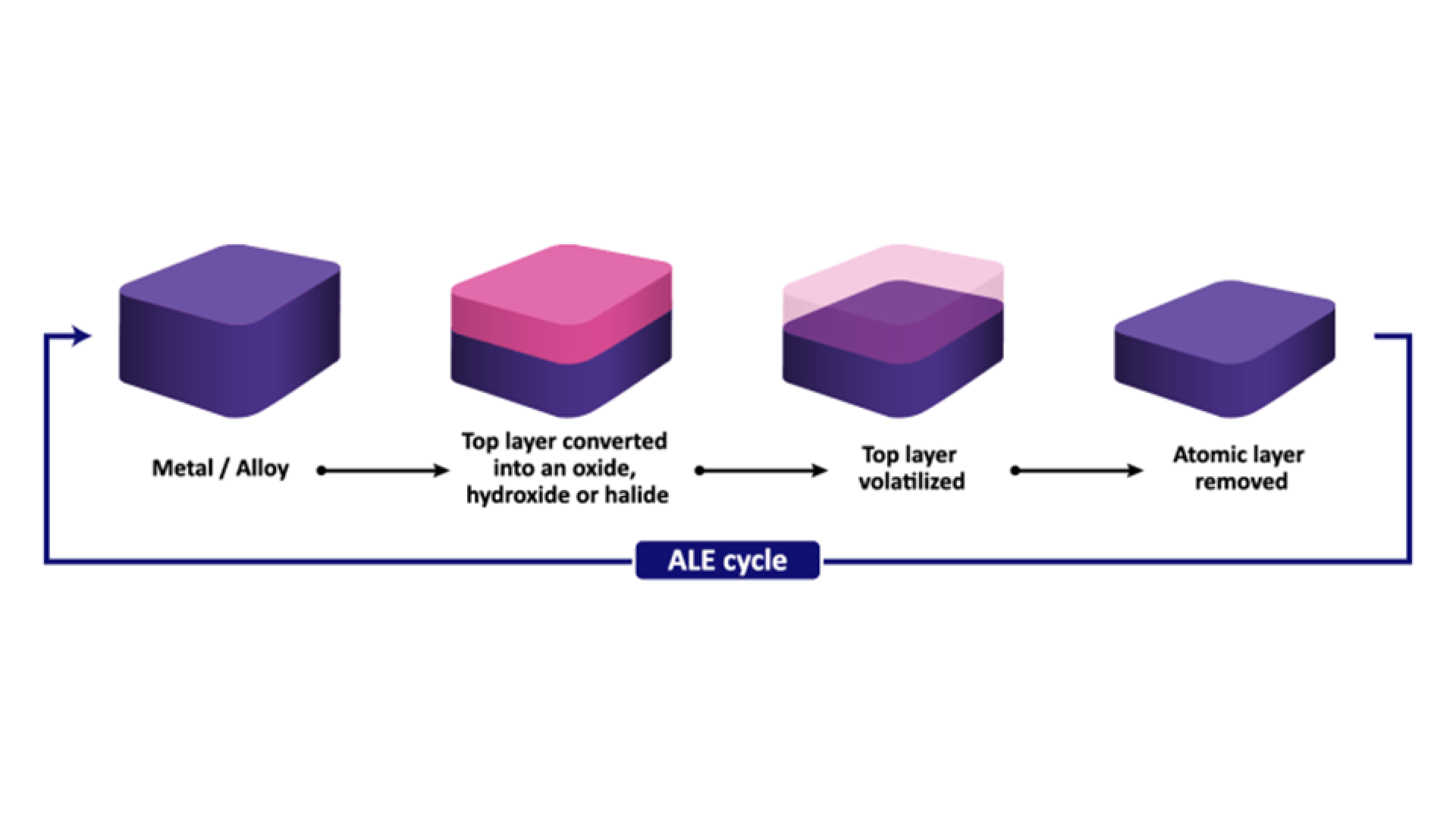
ALE cycle_figure 1
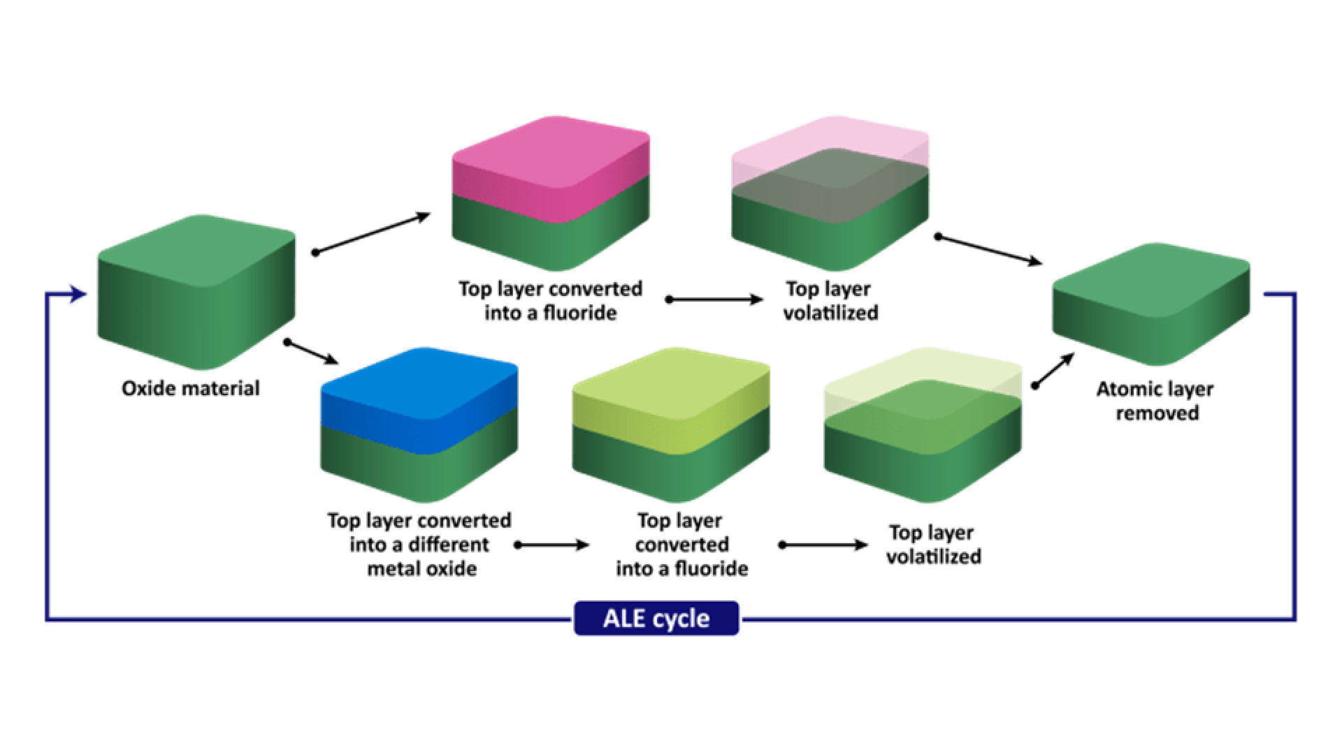
atomic layer etching_figure 2
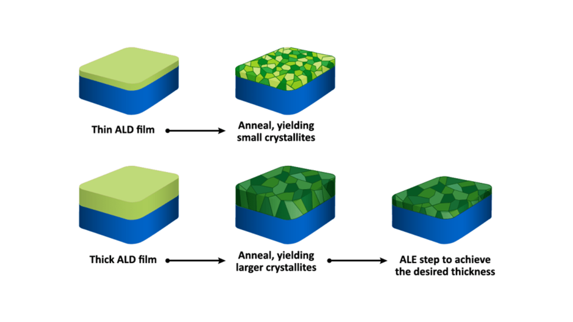
atomic layer etching _figure 3
More blogs
-
LOW-K INTERMETAL DIELECTRICS
By Robert Ridgeway, Senior R&D Manager, Product discovery, Versum Materials, EMD Electronics
Low-k Intermetal Dielectrics (ILD) have evolved from dense, single precursor based oxides to porous, structural and porogen based Low-k films. This blog discusses about the needs, challenges and our new precursor innovation in developing a successful ILD process for next-generation devices.
Learn More02 Nov 2021
-
SELECTING A GASGUARD SYSTEM FOR CONTROLLING HEATED SPECIALTY GASES
We recommend our new GASGUARD eV Temperature Control System! This blog reveals features and benefits of our new Temperature Control System.
Learn More02 Nov 2021
-
WORKING WITH CUSTOMERS TO DEVELOP NEW MOLECULES
By Anu Mallikarjunan, Global Marketing Manager, Planarization Global Business, EMD Electronics
As a leading innovation-driven electronic material supplier, we are committed to stretching the boundaries of science and technology in the semiconductor industry. In this blog, Anupama discusses the challenges we accepted, the steps we took, and the promising molecules we developed!
Learn More02 Nov 2021
-
ALD in Confined Spaces
In 3D vertical memory, active and electrode materials are layered inside deep vias with aspect ratios greater than 40:1. In previous posts, we’ve talked about how atomic layer deposition (ALD), a layer-by-layer, self-saturating chemical deposition process, can fill these types of structures.
Learn More14 Jan 2020
-
Leakage Variation with Aspect Ratio in ALD High-k ZrO2 Dielectrics
By Martin McBriarty, Scientific Manager, Intermolecular, EMD electronics
This blog summarizes the presentation given by Dr. Martin McBriarty on Atomic Layer Deposition in high-aspect-ratio-spaces, exploring how a material’s properties may change as the material goes into deep features and how we use a high-aspect ratio (HAR) test vehicle to investigate this behavior.
Learn More02 Nov 2021
-
Accelerating Analog AI R&D for Neuromorphic Computing Takes Intelligence
By Ganesh Panaman, Head of Intermolecular, EMD electronics
While artificial intelligence (AI) algorithms can be embedded in digital vonNeumann ICs, excessive size and energy consumption represents a significant barrier to the widespread adoption of such neuromorphic AI chips both at the “edge” and in the “cloud”.
Learn More11 Dec 2020
-
Industry’s First 4-Element ALD Chalcogenide-based OTS for 3D Memory Arrays
By Mario Laudato, Technical Manager, Intermolecular, EMD electronics
The semiconductor industry has been exploring the use of 3D crosspoint memory for years.
Learn More19 Aug 2020
-
Shedding new light onto the structure of ferroelectric hafnium oxide films
By Vijay Narasimhan, Manager, Early R&D & Incubator Programs, Intermolecular, EMD Electronics
Recently we discovered the presence of a transient crystal structure in hafnium oxide that forms just as it is heated above its crystallization temperature. We were able to “trap” this likely ferroelectric structure before it disappeared to make high performing ferroelectric capacitor.
Learn More02 Nov 2021
-
ASSAY MEANS PURITY, RIGHT?
By Suhas Ketkar, Head of Global Analytical Technology, EMD Electronics
Appropriate Examination of purity (assay) of a chemical is one of the major checkpoint in buyer-supplier relationship. In this blog, Dr. Suhas Ketkar reveals what is to 'assay' and how it is carried out for Organosilane and organometallic chemicals, also, the challenges in examining the purity.
Learn More02 Nov 2021