


TODAY, MORE AND MORE TRANSISTORS CAN FIT INTO THE SAME SURFACE AREA
There is still no end in sight for this development, because new technologies such as directed self-assembly (DSA) are further reducing component sizes.
Select your Market
{{ userContent.title }}

Integrated circuits are making electronic devices smaller and more powerful. Check out the technology Merck KGaA, Darmstadt, Germany and its partners have been working on in the field.
There is still no end in sight for this development, because new technologies such as directed self-assembly (DSA) are further reducing component sizes.
Back in 1965, Gordon Moore noticed that the number of transistors that could be mounted on an integrated circuit (chip) was doubling every year. “Moore’s Law,” as this observation came to be known, still applies today, more than 50 years later.
“This law has formed the foundations of the semiconductor industry ever since,” says Ralph Dammel, a chemist who has been working on chip development for nearly 30 years, initially at AZ Electronic Materials and now at Merck KGaA, Darmstadt, Germany, ever since its acquisition of AZ. Thanks to people like Dammel, circuits the size of a postage stamp can now accommodate nearly as many elements as there are people on earth — about seven billion.

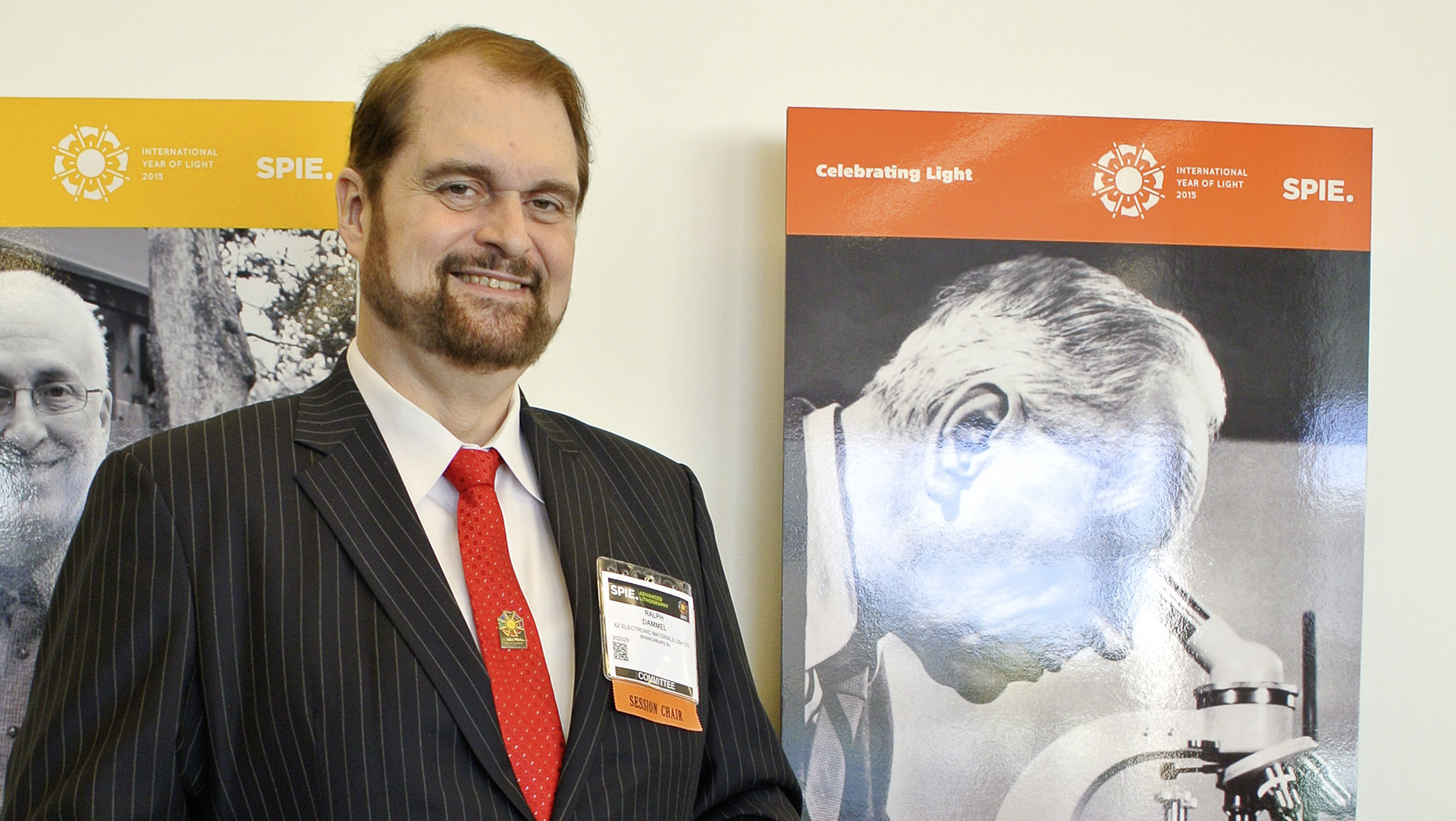
Ralph Dammel works in chip development at Merck KGaA, Darmstadt, Germany.
This incredible density largely results from the fact that today chips are no longer soldered; instead, they are manufactured in a process that closely resembles the traditional way a photograph used to be developed. Specifically, light is the tool that is used to create the circuits on silicon. The wavelengths of light are like wrench widths, and the finer the tool, the finer the structures that can be manipulated with that tool.
DSA already enables us to achieve a line width of 12.5 nanometers today.
Merck KGaA, Darmstadt, Germany
Blue has a short wavelength in the spectrum of visible light — around 435 nanometers (billionths of a millimeter). A human hair is just over 50,000 nanometers thick; compared with blue light, it’s like a tree trunk. Blue light was used as a tool to manufacture the first chips. And it was obvious that if this tool was refined it could produce even smaller structures. Engineers therefore started moving into the invisible region of the spectrum. These days they use wavelengths of 193 nanometers. “When you go below this 193-nanometer scale, it becomes impossible to build optical systems that allow light to pass through,” says Dammel.
Nevertheless, the use of this technology and additional tricks during the exposure of the structures have made it possible to mass-produce chips that have a structural width of only 45 nanometers. This width accommodates between 50 and just under 100 atoms — the smallest components of chemical compounds. It now becomes clear just how close chip production has come to its physical limits. Such chips, which are now mass-produced, function reliably for years and have enabled the creation of ever smaller and more powerful microprocessors. These processors can be found in every cell phone — and also in every washing machine and automobile. Their tiny dimensions and low unit costs offer an initial preview of the Internet of Things, in which virtually every object will contain a microprocessor that can also be wirelessly networked.
Economists such as Jeremy Rifkin believe this forms the foundations of a zero marginal cost society — a scenario in which, for the first time in human history, greater performance comes at virtually no extra cost. Internet banking and free access to most of the world’s knowledge are visible manifestations of this future, which in turn will be largely shaped by how Moore’s Law continues to unfold.
One aspect of this development will be the further reduction of the wavelength to 13.5 nanometers, which is a lot less than a tenth of the current “tool size.” At the same time, the drawbacks of exposure using these soft X-rays are considerable. For one thing, the cost of the equipment needed is more than three times as high as that of today’s technology. In addition, the production rate per hour is just one quarter of the current rate. “This of course makes the new chips much more expensive,” says Dammel. Yet he also knows how a new technology can solve this problem.

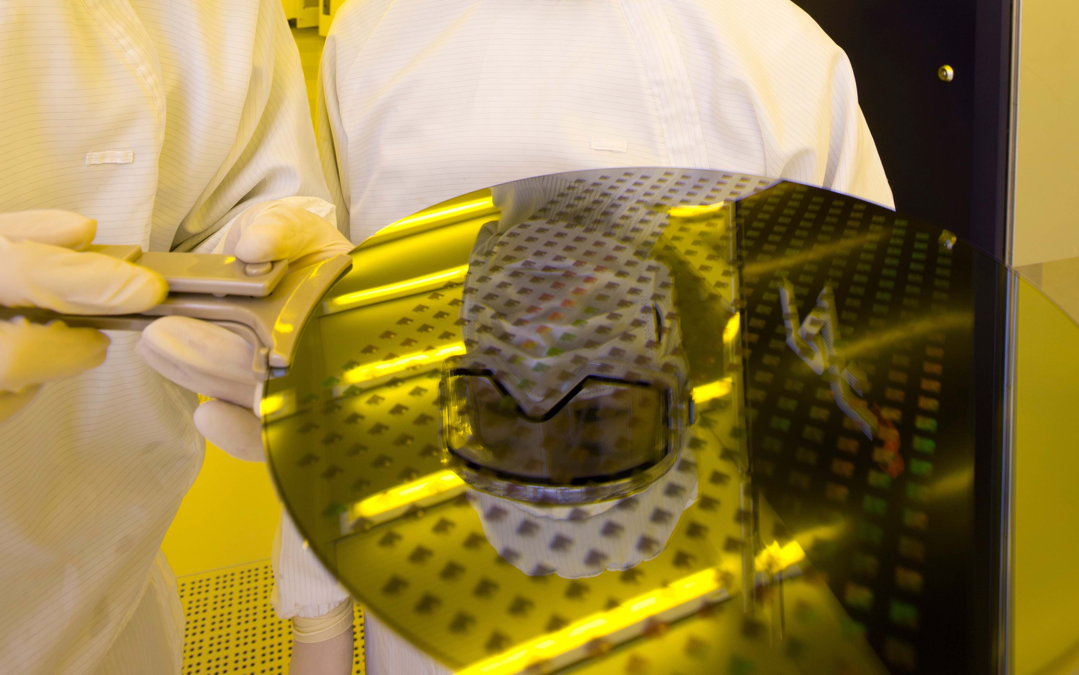
The starting materials for chip manufacturing are like wafers — thin, absolutely smooth slices of ultra-pure silicon on which dozens of chips are created simultaneously.
A new innovative technology jointly developed by Merck KGaA, Darmstadt, Germany and IBM features a material that can form the fine-line chip structures itself. This method, which is known as directed self-assembly (DSA), uses plastics (polymers) with a varied range of special properties. When two of these “block copolymers” are mixed in equal amounts, they form a structure made of narrow lamellae.

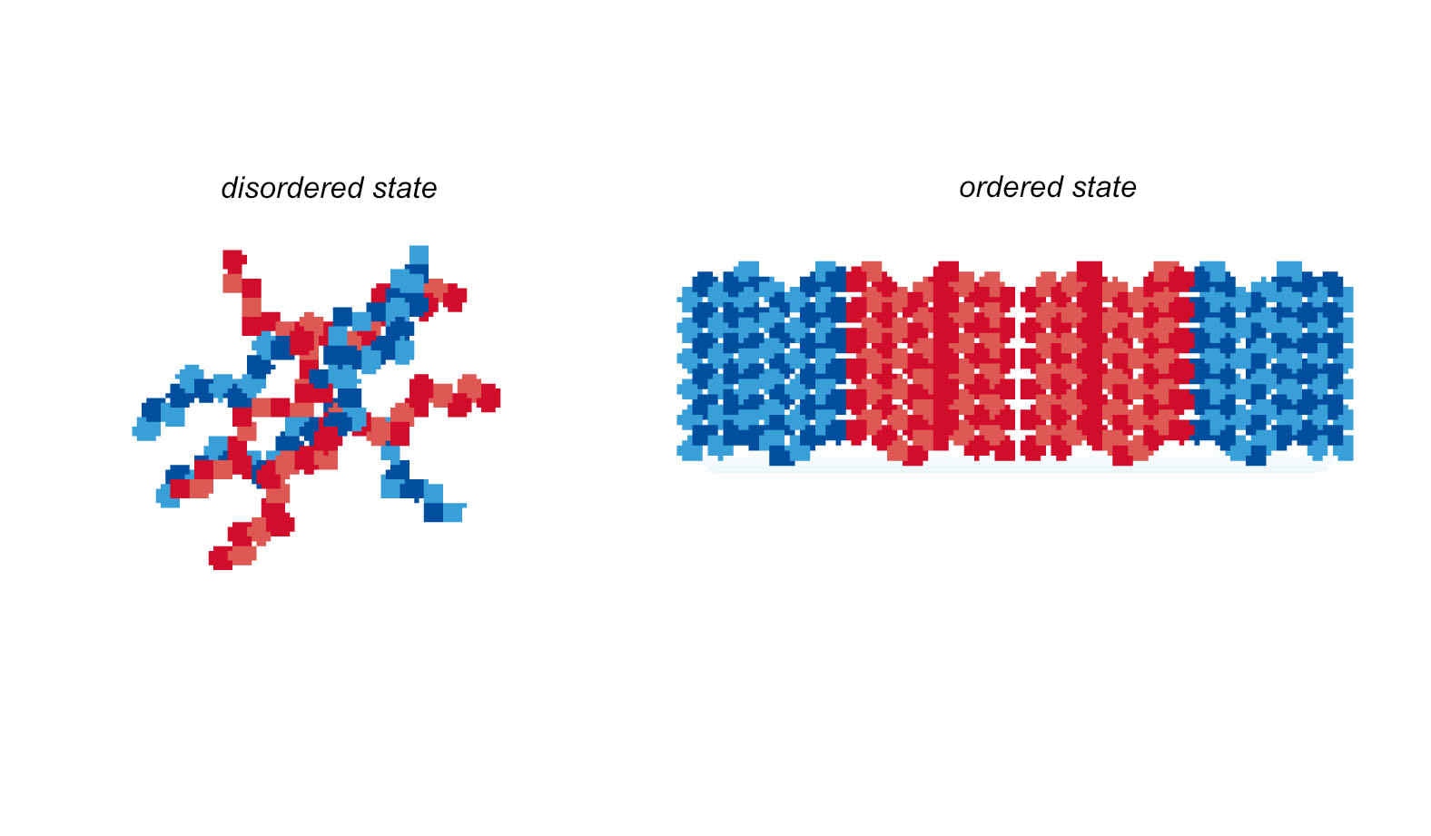
Under certain chip conditions, these block copolymers arrange themselves into uniform shapes. They form foundations for the extremely fine transistors and printed conductors of future computer chips.
The self-assembly aspect of this technology radically surpasses the previous phase of development, which relied on using ever-shorter wavelengths. “Our current workhorse is a very simple polymer that enables us to achieve a line width of 12.5 nanometers,” says Dammel. “However, we are also developing products that will enable us to produce lines with widths as narrow as six nanometers.”
This production method is not yet ready for mass application, but when it is, it will take the CMOS semiconductor technology down to its limit of five nanometers. This breakthrough is expected to be achieved in 2020 — probably with the help of DSA technology, which will be used in mass-production operations for the first time in 2016. Even smaller and more powerful processors will then accelerate developments further.